Get started with Agilex™ 3 SoC FPGA(M16A) SOM Development Platform
Unpacking
Remove the Development Platform from box and place above the ESD free area. Use anti-static pad/mat with proper grounding to place the Development Platform. Also make sure that, below deliverables are received without any physical damage.
Development kit contains:
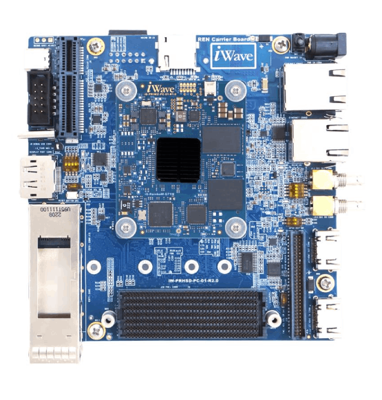
Agilex 3 SoC FPGA(M16A) SOM Development Platform
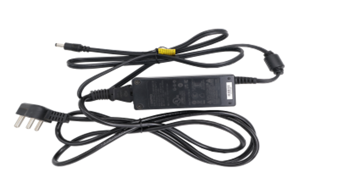
12V, 5A Power Supply
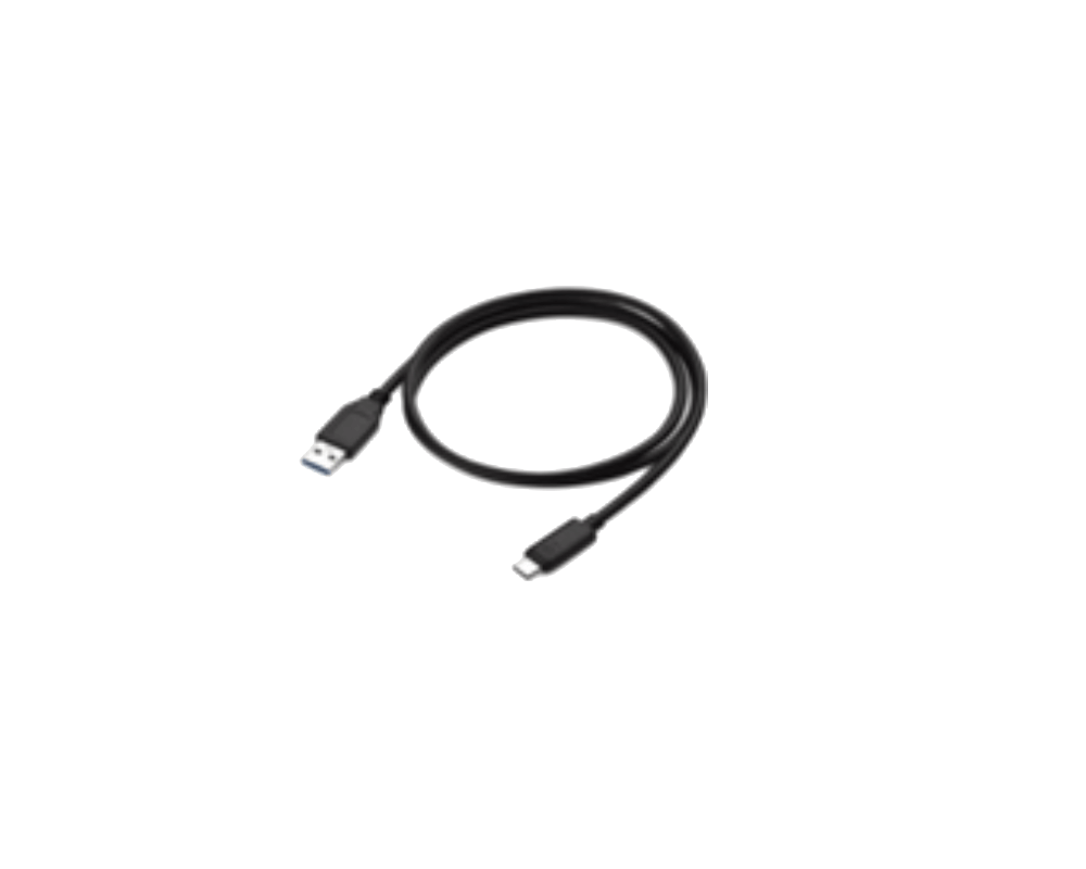
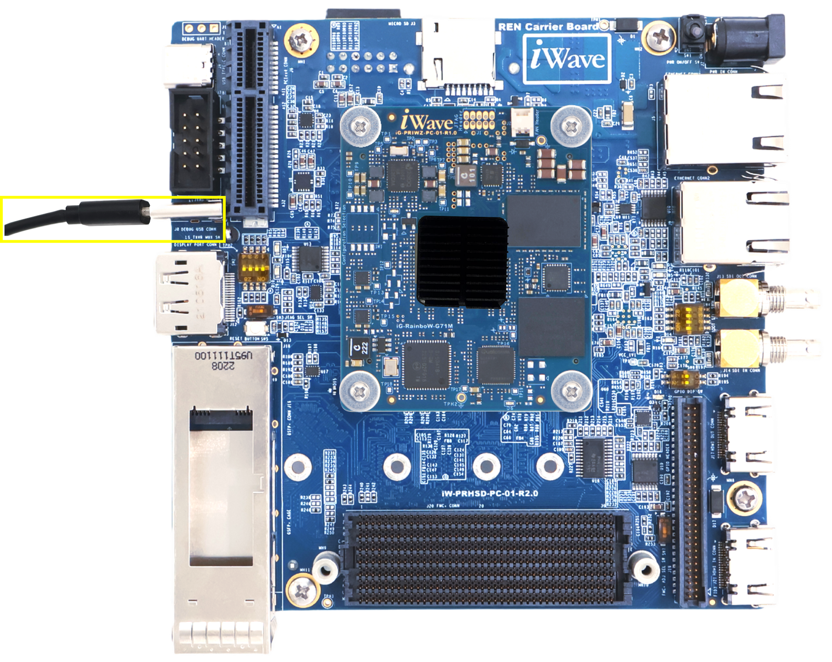
USB Debug cable
Agilex 3 SoC FPGA(M16A) SOM Development Platform
12V, 5A Power Supply
USB Debug cable
Get to know
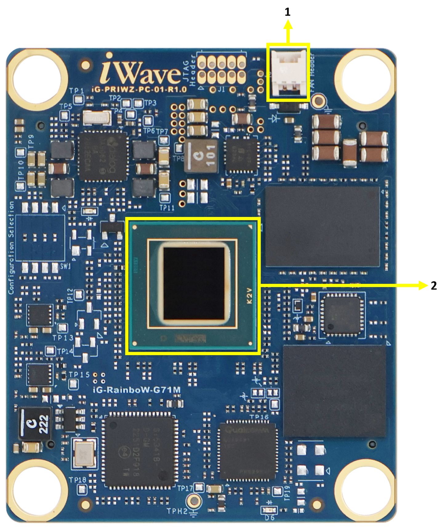
Agilex 3 SoC FPGA(M16A) SOM – Top view
Fan Connector
Agilex 3 SoC FPGA (M16A)
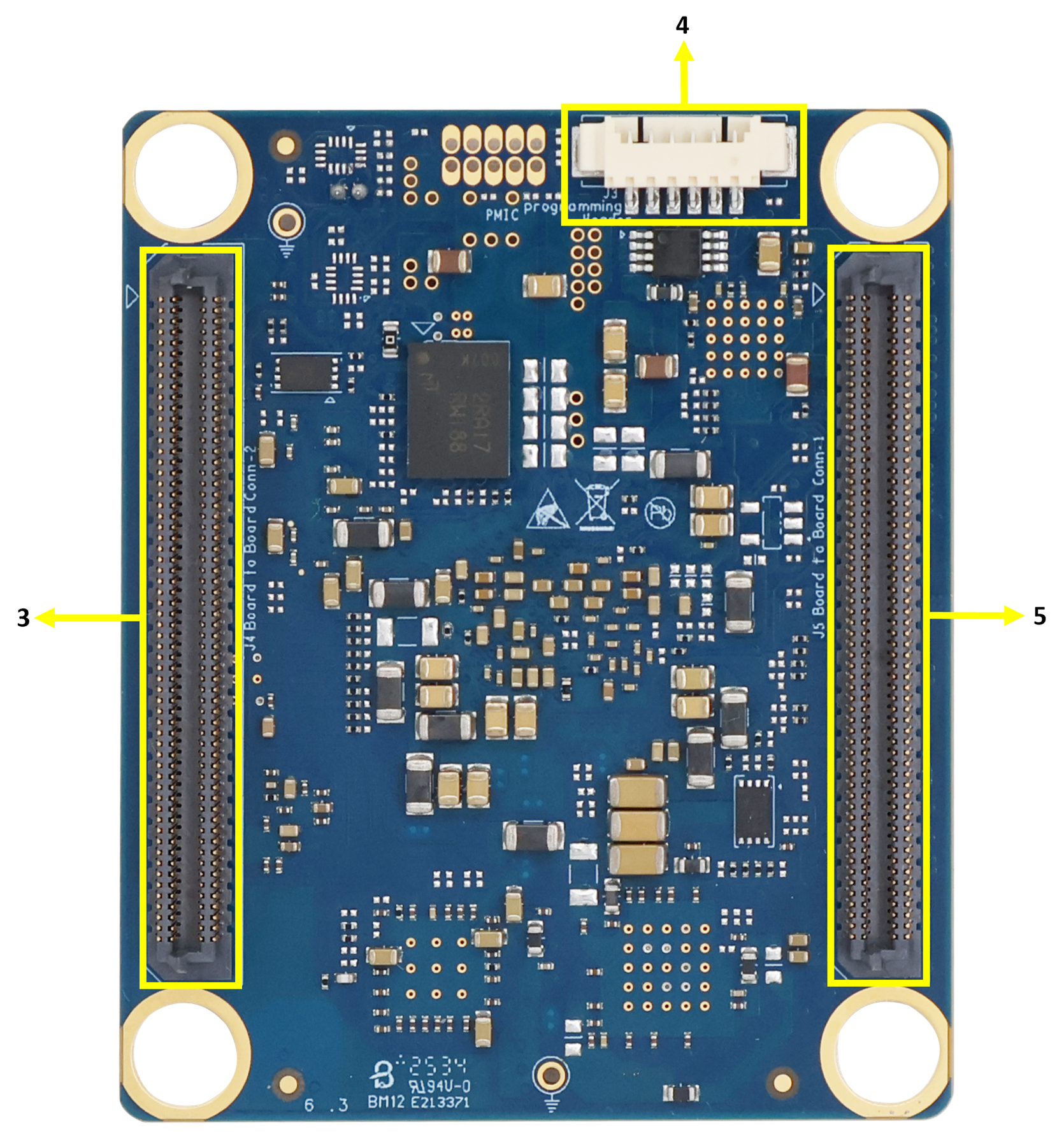
Agilex 3 SoC FPGA(M16A) SOM – Bottom view
3. Board to Board connector 2 4. PMIC Programing Header 5. Board to Board connector 1
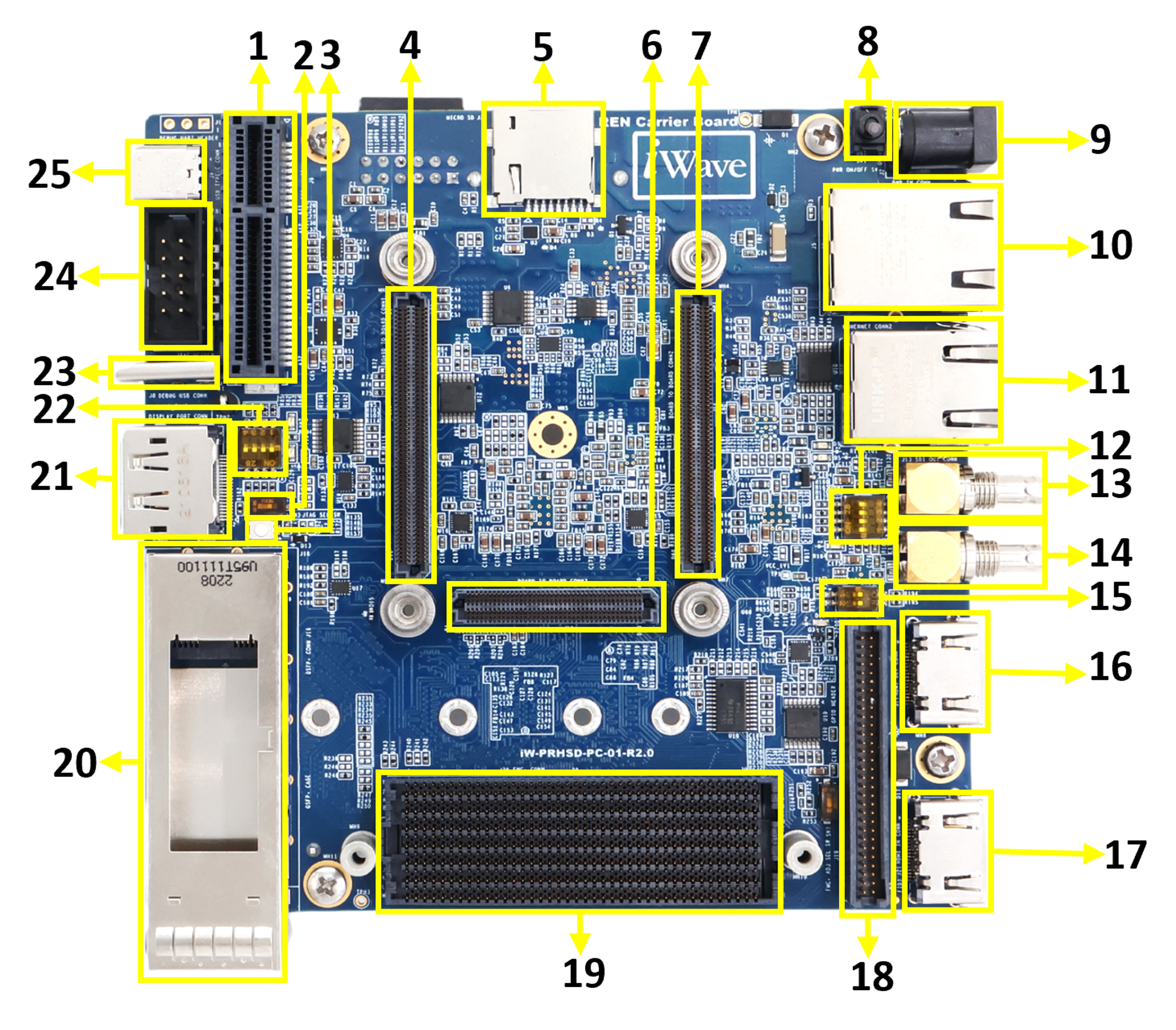
Agilex 3 SoC FPGA(M16A) Development Platform – Top view
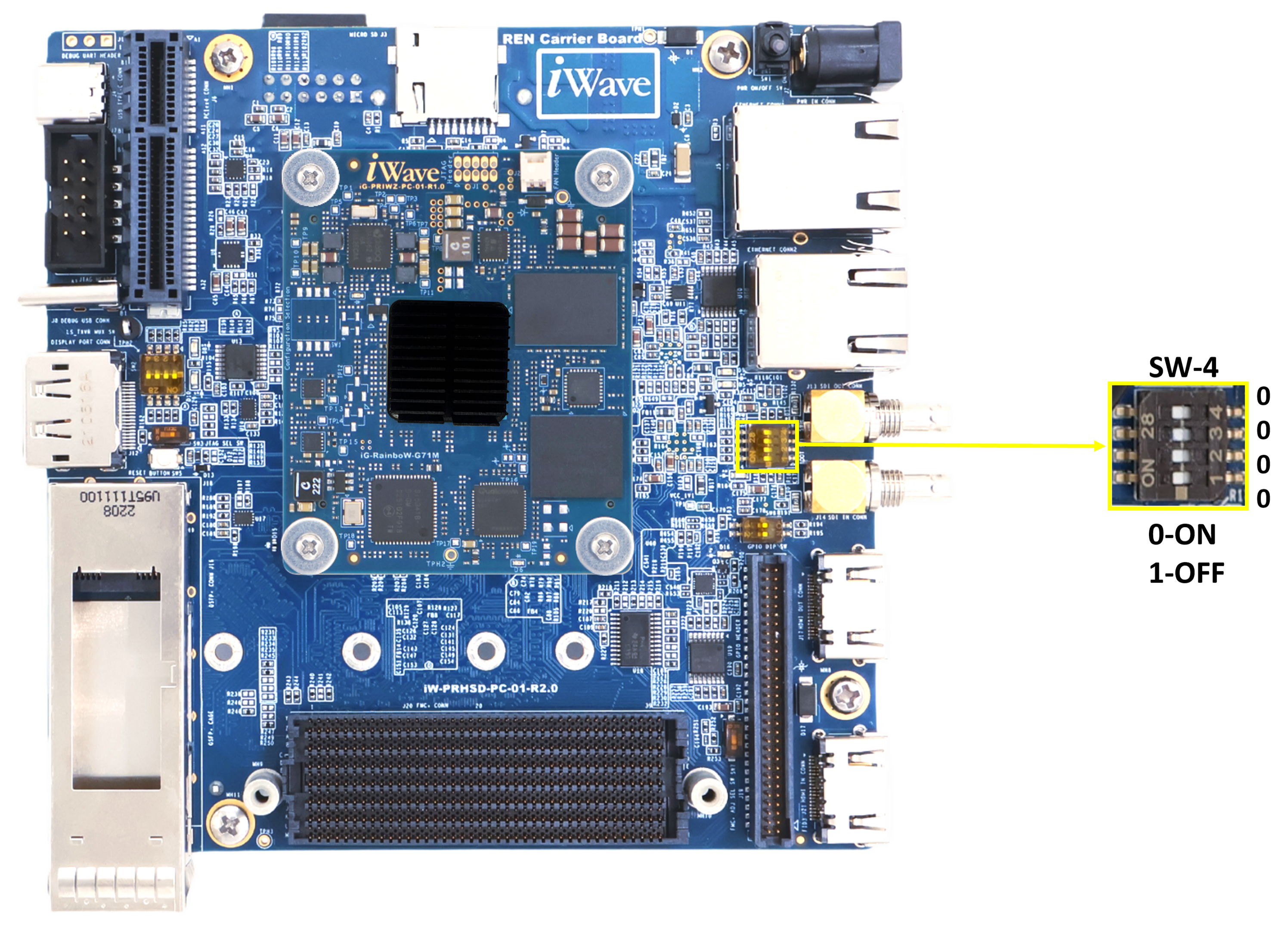
1. PCIe x4 Connector 2. JTAG SEL Switch 3. RESET Switch 4. Board to Board Connector 1 5. Micro SD Connector * 6. Board to Board Connector 3** 7. Board to Board Connector 2 8. ON/OFF Switch 9. Power Jack 10. SGMII Ethernet Jack 11. RGMII Ethernet Jack 12. Boot Media Selection 13. SDI OUT**
14. SDI IN** 15. GPIO DIP Switch 16. HDMI OUT** 17. HDMI IN** 18. GPIO Header 19. FMC+ Connector 20. QSFP Connector** 21. Display Port 22. LS_MUX/PCIE_SEL-Switch 23. Debug UART Connector 24. JTAG Connector 25. USB Type C Connector
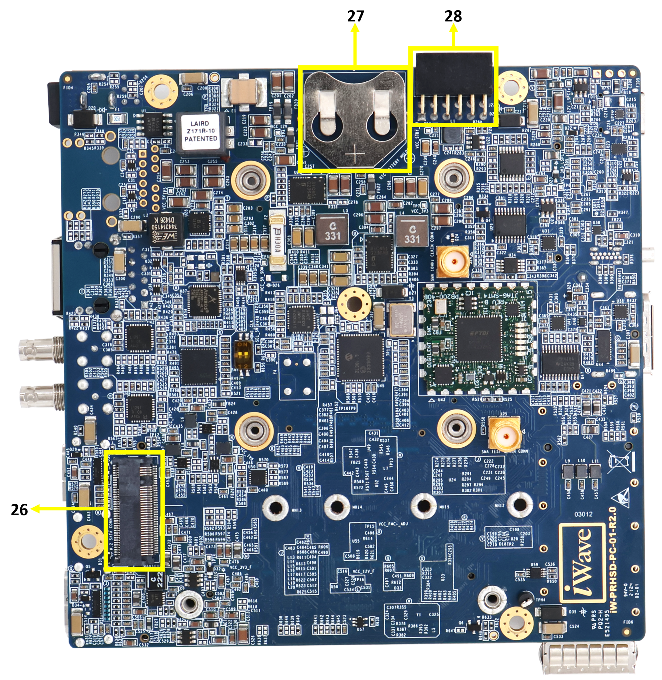
Agilex 3 SoC FPGA(M16A) Development Platform – Bottom view
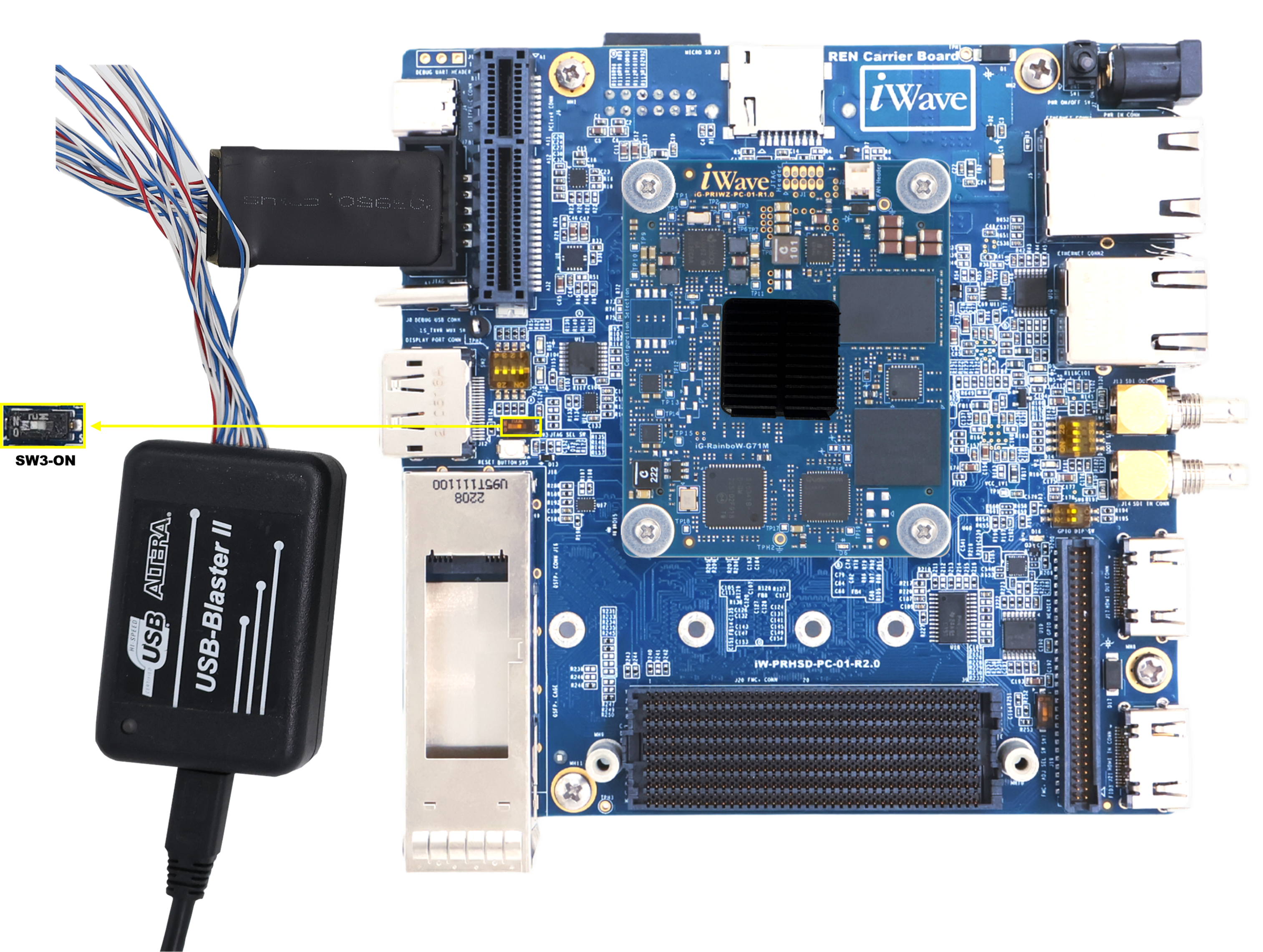
iG-RainboW-G71D Agilex 3 SoC FPGA(M16A) SOM Development platform support JTAG interface for FPGA Programming and debugging. Use the USB Blaster to connect Carrier Board. Ensure that Switch-3 on the carrier board is turned ON.
Example USB Blaster which is tested with this Platform is mentioned below. USB Blaster-2 Part Number : PL-USB2-BLASTER from INTEL
Powering ON
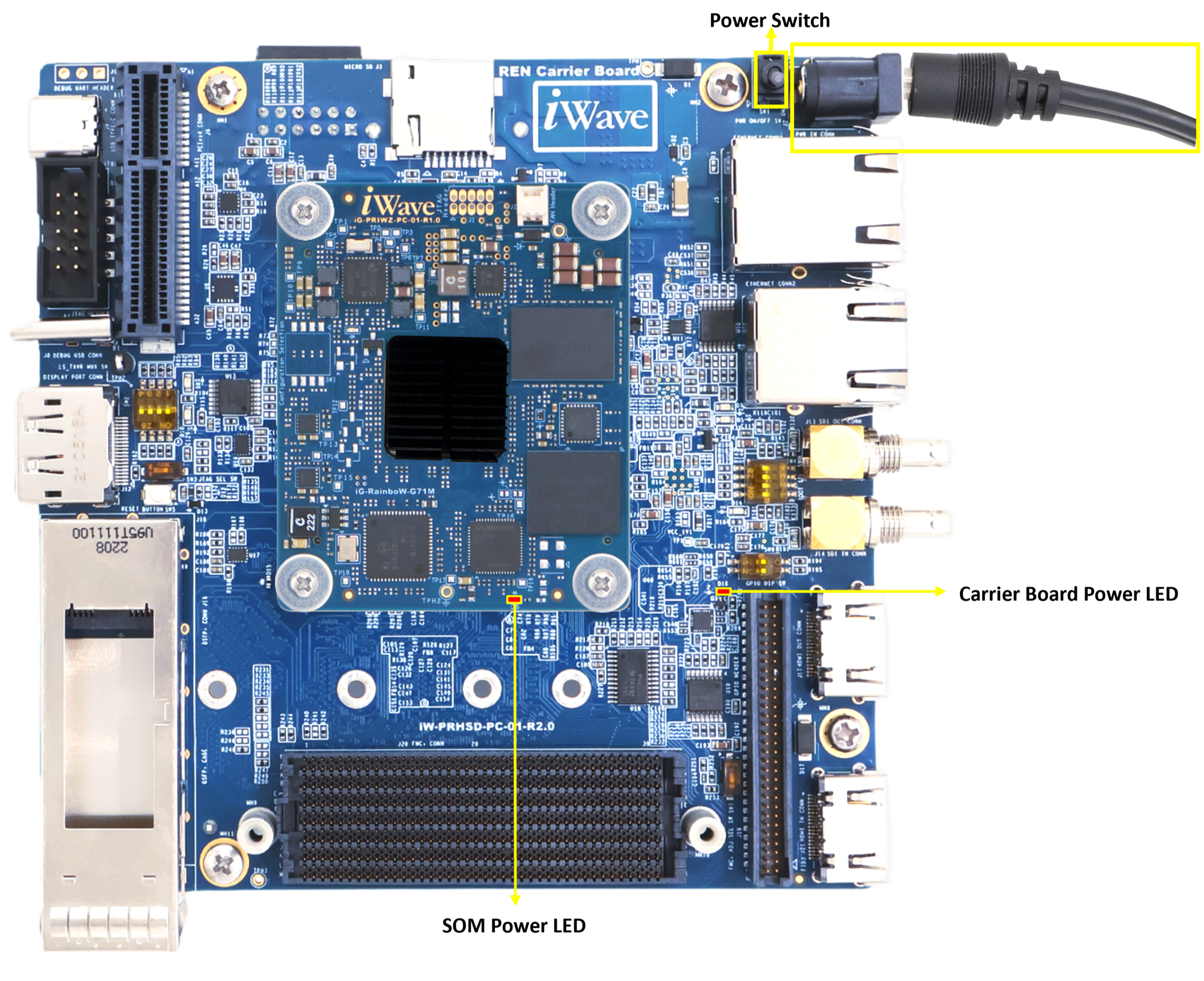
Connect the Power supply plug to the Power connector (J2) of the Development platform as shown below and switch ON the power supply. Once power is applied to the Development platform, the power LED in the Development platform will glow as shown in the below image.
Warning:
Do not try to connect any other Power Supply other than supplied along with Agilex 3 SoC FPGA(M16A) SOM Development Platform.
Do not plug or remove the Agilex 3 SoC FPGA(M16A) SOM from carrier board with live power.
Contact iWave, if power LEDs are not glowing.
Test Environment setup
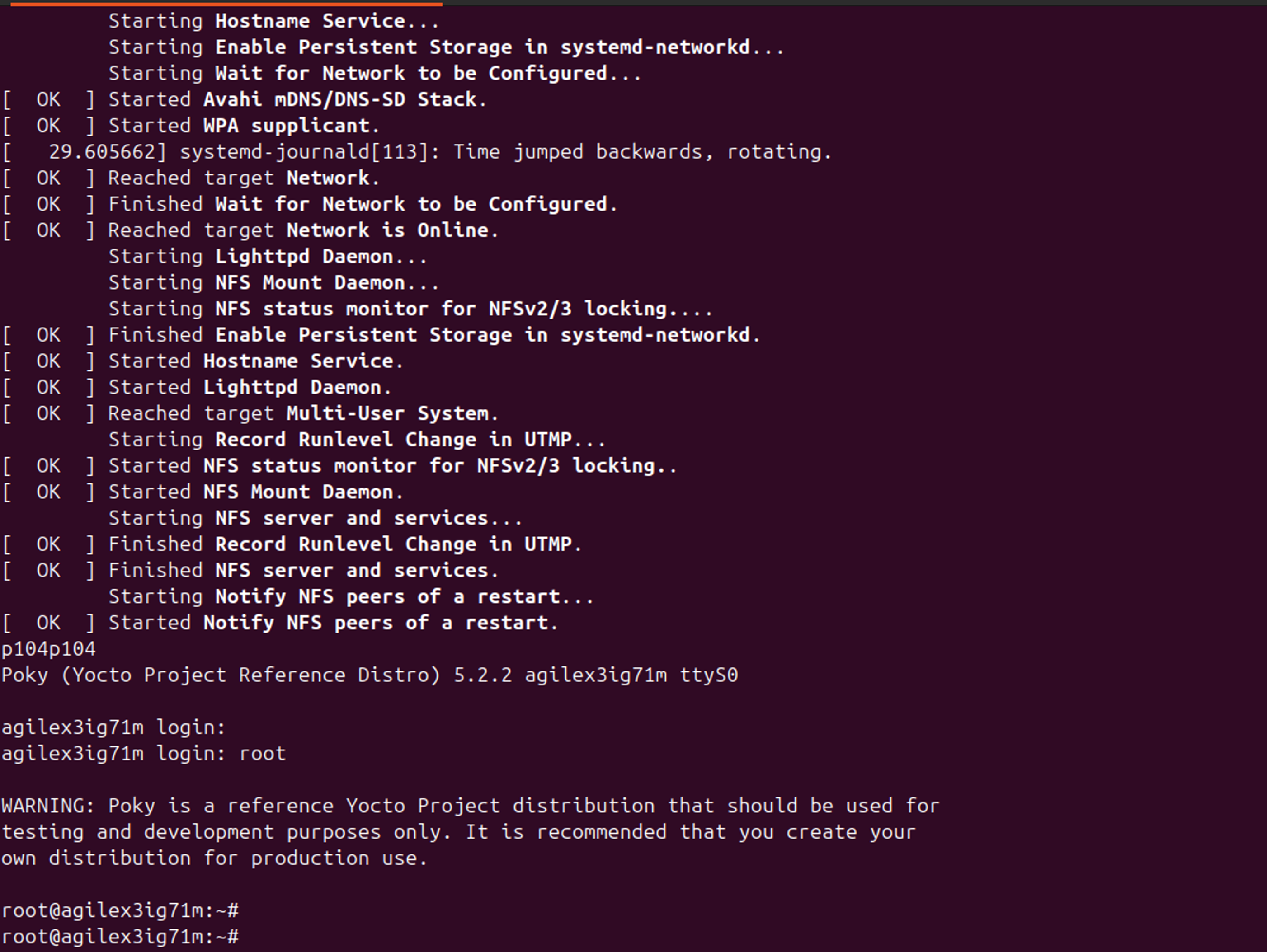
Command Prompt
Contact Us
We appreciate you contacting iWave. Our representative will get in touch with you soon!